- 您现在的位置:买卖IC网 > Sheet目录3882 > PIC16F87T-E/ML (Microchip Technology)IC MCU FLASH 4KX14 EEPROM 28QFN
86
8008H–AVR–04/11
ATtiny48/88
Notes:
1. MAX
= 0xFF
Bits 2:0 – CS0[2:0]: Clock Select
The three Clock Select bits select the clock source to be used by the Timer/Counter.
If external pin modes are used for the Timer/Counter0, transitions on the T0 pin will clock the
counter even if the pin is configured as an output. This feature allows software control of the
counting.
11.8.2
TCNT0 – Timer/Counter Register
The Timer/Counter Register gives direct access, both for read and write operations, to the
Timer/Counter unit 8-bit counter. Writing to the TCNT0 Register blocks (removes) the Compare
Match on the following timer clock. Modifying the counter (TCNT0) while the counter is running,
introduces a risk of missing a Compare Match between TCNT0 and the OCR0x Registers.
11.8.3
OCR0A – Output Compare Register A
The Output Compare Register A contains an 8-bit value that is continuously compared with the
counter value (TCNT0). A match can be used to generate an Output Compare interrupt.
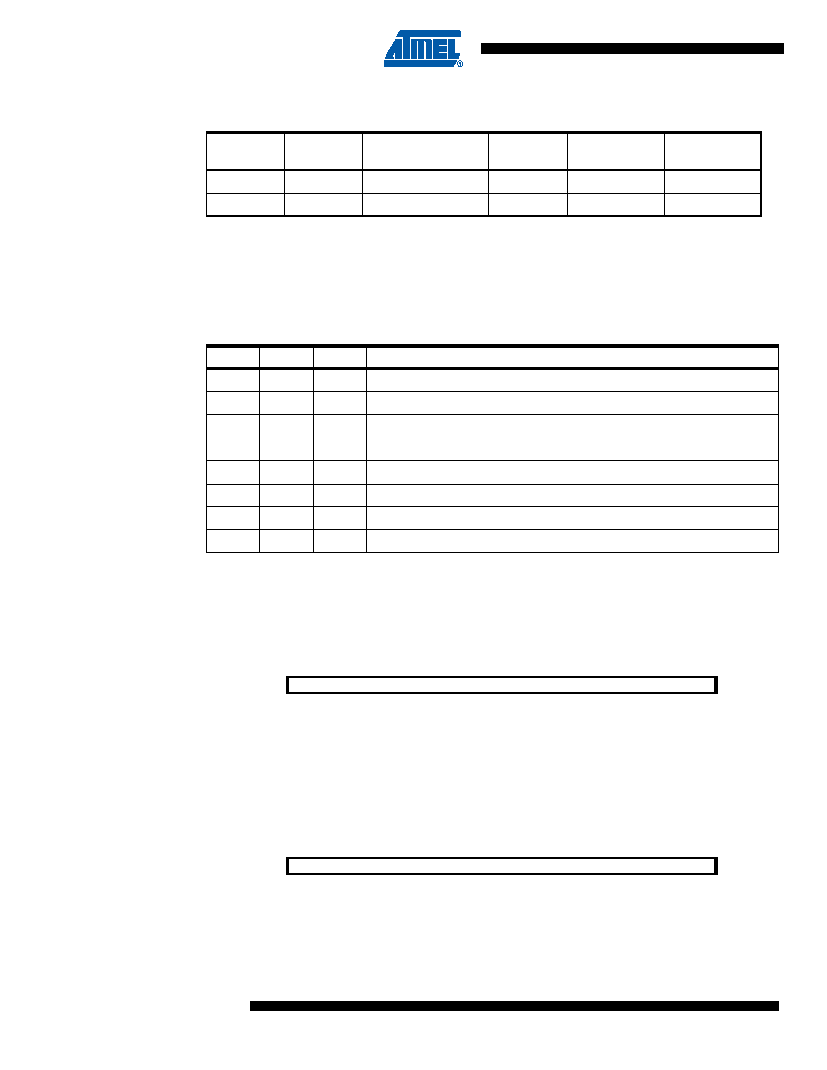
Table 11-2.
CTC Mode Bit Description
Mode
CTC0
Timer/Counter
Mode of Operation
TOP
Update of
OCRx at
TOV Flag
Set on
0
Normal
0xFF
Immediate
MAX
1
CTC
OCRA
Immediate
MAX
Table 11-3.
Clock Select Bit Description
CS02
CS01
CS00
Description
0
No clock source (Timer/Counter stopped)
00
1
clkI/O (No prescaling)
01
0
clkI/O/8 (From prescaler)
01
1
clkI/O/64 (From prescaler)
10
0
clkI/O/256 (From prescaler)
10
1
clkI/O/1024 (From prescaler)
1
0
External clock source on T0 pin. Clock on falling edge.
1
External clock source on T0 pin. Clock on rising edge.
Bit
7
654
32
10
TCNT0[7:0]
TCNT0
Read/Write
R/W
Initial Value
0
Bit
7
654
32
10
OCR0A[7:0]
OCR0A
Read/Write
R/W
Initial Value
0
发布紧急采购,3分钟左右您将得到回复。
相关PDF资料
PIC16F87-E/ML
IC MCU FLASH 4KX14 EEPROM 28QFN
PIC18LF4320-I/ML
IC MCU FLASH 4KX16 EEPROM 44QFN
PIC16F77T-I/PTG
IC MCU FLASH 8KX14 W/AD 44TQFP
PIC16LF1933-I/SO
IC PIC MCU FLASH 4K 28-SOIC
PIC16C54C-20I/SO
IC MCU OTP 512X12 18SOIC
PIC16LF726-I/SO
IC PIC MCU FLASH 8K 1.8V 28-SOIC
PIC12CE673-10/P
IC MCU OTP 1KX14 A/D&EE 8DIP
PIC16F726-I/SO
IC PIC MCU FLASH 8KX14 28-SOIC
相关代理商/技术参数
PIC16F87T-E/SO
功能描述:8位微控制器 -MCU 20MHz 4K Flash RoHS:否 制造商:Silicon Labs 核心:8051 处理器系列:C8051F39x 数据总线宽度:8 bit 最大时钟频率:50 MHz 程序存储器大小:16 KB 数据 RAM 大小:1 KB 片上 ADC:Yes 工作电源电压:1.8 V to 3.6 V 工作温度范围:- 40 C to + 105 C 封装 / 箱体:QFN-20 安装风格:SMD/SMT
PIC16F87T-E/SS
功能描述:8位微控制器 -MCU 20MHz 4K Flash RoHS:否 制造商:Silicon Labs 核心:8051 处理器系列:C8051F39x 数据总线宽度:8 bit 最大时钟频率:50 MHz 程序存储器大小:16 KB 数据 RAM 大小:1 KB 片上 ADC:Yes 工作电源电压:1.8 V to 3.6 V 工作温度范围:- 40 C to + 105 C 封装 / 箱体:QFN-20 安装风格:SMD/SMT
PIC16F87T-I/ML
功能描述:8位微控制器 -MCU 7KB 368 RAM 16 I/O RoHS:否 制造商:Silicon Labs 核心:8051 处理器系列:C8051F39x 数据总线宽度:8 bit 最大时钟频率:50 MHz 程序存储器大小:16 KB 数据 RAM 大小:1 KB 片上 ADC:Yes 工作电源电压:1.8 V to 3.6 V 工作温度范围:- 40 C to + 105 C 封装 / 箱体:QFN-20 安装风格:SMD/SMT
PIC16F87T-I/SO
功能描述:8位微控制器 -MCU 7KB 368 RAM 16 I/O RoHS:否 制造商:Silicon Labs 核心:8051 处理器系列:C8051F39x 数据总线宽度:8 bit 最大时钟频率:50 MHz 程序存储器大小:16 KB 数据 RAM 大小:1 KB 片上 ADC:Yes 工作电源电压:1.8 V to 3.6 V 工作温度范围:- 40 C to + 105 C 封装 / 箱体:QFN-20 安装风格:SMD/SMT
PIC16F87T-I/SS
功能描述:8位微控制器 -MCU 7KB 368 RAM 16 I/O RoHS:否 制造商:Silicon Labs 核心:8051 处理器系列:C8051F39x 数据总线宽度:8 bit 最大时钟频率:50 MHz 程序存储器大小:16 KB 数据 RAM 大小:1 KB 片上 ADC:Yes 工作电源电压:1.8 V to 3.6 V 工作温度范围:- 40 C to + 105 C 封装 / 箱体:QFN-20 安装风格:SMD/SMT
PIC16F882-E/ML
功能描述:8位微控制器 -MCU 3.5KB Enh FLSH 128 RAM RoHS:否 制造商:Silicon Labs 核心:8051 处理器系列:C8051F39x 数据总线宽度:8 bit 最大时钟频率:50 MHz 程序存储器大小:16 KB 数据 RAM 大小:1 KB 片上 ADC:Yes 工作电源电压:1.8 V to 3.6 V 工作温度范围:- 40 C to + 105 C 封装 / 箱体:QFN-20 安装风格:SMD/SMT
PIC16F882-E/SO
功能描述:8位微控制器 -MCU 3.5KB Enh FLSH 128 RAM RoHS:否 制造商:Silicon Labs 核心:8051 处理器系列:C8051F39x 数据总线宽度:8 bit 最大时钟频率:50 MHz 程序存储器大小:16 KB 数据 RAM 大小:1 KB 片上 ADC:Yes 工作电源电压:1.8 V to 3.6 V 工作温度范围:- 40 C to + 105 C 封装 / 箱体:QFN-20 安装风格:SMD/SMT
PIC16F882-E/SP
功能描述:8位微控制器 -MCU 3.5KB Enh FLSH 128 RAM RoHS:否 制造商:Silicon Labs 核心:8051 处理器系列:C8051F39x 数据总线宽度:8 bit 最大时钟频率:50 MHz 程序存储器大小:16 KB 数据 RAM 大小:1 KB 片上 ADC:Yes 工作电源电压:1.8 V to 3.6 V 工作温度范围:- 40 C to + 105 C 封装 / 箱体:QFN-20 安装风格:SMD/SMT